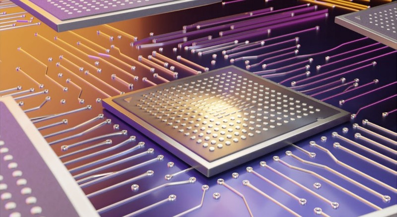
3D IC and 2.5D IC Packaging Market Changing the Industries
Introduction to 3D IC and 2.5D IC Packaging
The world of integrated circuit (IC) packaging technology has witnessed significant advancements in recent years, and one of the most groundbreaking developments is the emergence of 3D IC and 2.5D IC packaging.
These packaging techniques have revolutionized the way electronic components are stacked and interconnected, unlocking new possibilities for various industries.
In this article, we will delve into the basics of 3D IC and 2.5D IC packaging, explore their advantages, applications in different industries, and understand the impact they have on the medical devices sector.
Understanding the basics of IC packaging technology
Before we dive into the specifics of 3D IC and 2.5D IC packaging, it is essential to grasp the fundamentals of IC packaging technology. IC packaging is the process of enclosing electronic components, such as microchips, in protective casings to ensure their functionality and reliability.
Traditional IC packaging involves the use of single-layer packaging techniques, where components are placed side by side on a single plane. However, with the advent of 3D IC and 2.5D IC packaging, a new dimension has been added to this process.
Advantages of 3D IC and 2.5D IC Packaging
The adoption of 3D IC and 2.5D IC packaging has brought forth numerous advantages for the electronics industry. Firstly, these techniques allow for higher component density, enabling the integration of more functionality within a smaller footprint.
This is particularly beneficial for industries where size constraints are a concern, such as wearable devices and mobile technology.
Secondly, 3D IC and 2.5D IC packaging enhance performance and speed by reducing signal propagation delays. By stacking components vertically and minimizing interconnect lengths, the distance that signals need to travel is significantly reduced, resulting in improved overall system performance.
This advantage is particularly crucial in industries that rely heavily on data processing and real-time operations, such as telecommunications and automotive.
Another advantage of 3D IC and 2.5D IC packaging is increased power efficiency. By reducing interconnect lengths and optimizing power distribution, these packaging techniques minimize power losses and improve energy efficiency. This is a crucial factor in industries striving for sustainability and energy conservation, such as renewable energy and IoT devices.
Applications of 3D IC and 2.5D IC Packaging in different industries
The versatility of 3D IC and 2.5D IC packaging has enabled their application in a wide range of industries. In the consumer electronics sector, these packaging techniques have revolutionized the design and functionality of smartphones, tablets, and smartwatches.
The compact form factor of 3D IC and 2.5D IC packaging allows for sleeker and more lightweight devices without compromising performance.
In the automotive industry, 3D IC and 2.5D IC packaging have played a pivotal role in the development of advanced driver-assistance systems (ADAS) and autonomous vehicles.
These packaging techniques enable the integration of multiple sensors and processing units, facilitating real-time data analysis and decision-making for enhanced safety and driving experience.
The aerospace and defense sector has also benefited from 3D IC and 2.5D IC packaging. By utilizing these techniques, manufacturers can create compact and lightweight electronic systems for satellites, unmanned aerial vehicles (UAVs), and military equipment. This allows for more efficient use of limited space and increased payload capacity.
Impact of 3D IC and 2.5D IC Packaging on the medical devices industry
One industry that has witnessed a profound impact from 3D IC and 2.5D IC packaging is the medical devices sector. These packaging techniques have revolutionized the design and functionality of medical devices, enabling the development of more advanced and compact solutions.
In the field of implantable medical devices, such as pacemakers and neurostimulators, 3D IC and 2.5D IC packaging have allowed for the integration of multiple components within a smaller form factor. This not only improves patient comfort but also enables more precise and effective therapies.
Furthermore, 3D IC and 2.5D IC packaging have facilitated the development of portable medical devices, such as glucose monitors and wearable health trackers. The compact size and enhanced performance offered by these packaging techniques have made it possible to create devices that can be conveniently worn or carried by patients, enabling continuous monitoring and personalized healthcare.
Future prospects and trends in 3D IC and 2.5D IC Packaging
The future of 3D IC and 2.5D IC packaging looks promising, with several trends and advancements on the horizon. One notable trend is the integration of heterogeneous components within a single package.
This involves combining different types of chips, such as processors, memory, and sensors, into a compact and interconnected system. This integration allows for improved performance, reduced power consumption, and increased functionality.
Another emerging trend is the development of advanced cooling solutions for 3D IC and 2.5D IC packages. As the density of components increases, thermal management becomes a critical aspect.
Innovations in thermal interface materials and cooling techniques, such as microfluidic cooling, are expected to address this challenge and enable the efficient dissipation of heat generated by densely packed components.
Additionally, the adoption of fan-out wafer-level packaging (FOWLP) is gaining traction in the 3D IC and 2.5D IC packaging market. FOWLP offers a cost-effective solution for high-density packaging, as it eliminates the need for traditional wire bonding and flip-chip assembly. This technique allows for the integration of more components, reduces package size, and enhances signal integrity.
Challenges and limitations of 3D IC and 2.5D IC Packaging
While 3D IC and 2.5D IC packaging offer numerous advantages, they also come with their own set of challenges and limitations. One significant challenge is the complexity of design and manufacturing processes.
As the number of stacked layers and interconnects increases, the design and fabrication become more intricate, requiring advanced engineering expertise and specialized equipment.
Another challenge is the potential for thermal issues in densely packed 3D IC and 2.5D IC packages. The proximity of components can lead to heat buildup, which may affect performance and reliability. Effective thermal management techniques, as mentioned earlier, are crucial to address this challenge.
Furthermore, the cost of implementing 3D IC and 2.5D IC packaging can be a limiting factor for widespread adoption. The additional manufacturing steps and specialized equipment required for these packaging techniques can result in higher production costs.
However, as the technology matures and economies of scale are achieved, the cost barrier is expected to decrease.
Key players in the 3D IC and 2.5D IC Packaging market
The global 3D IC and 2.5D IC packaging market is highly competitive, with several key players driving innovation and market growth. Some of the major players in this industry include TSMC, Samsung Electronics, Intel Corporation, and ASE Group.
These companies invest heavily in research and development to push the boundaries of IC packaging technology and cater to the evolving needs of end-user industries.
Recent developments and innovations in IC packaging technology
The field of IC packaging technology is constantly evolving, with new developments and innovations being introduced regularly. One notable advancement is the use of through-silicon vias (TSVs) in 3D IC packaging.
TSVs are vertical interconnects that enable the transfer of signals and power between stacked layers. This technology has significantly improved the interconnect density and performance of 3D IC packages.
Another noteworthy innovation is the use of wafer-level chip-scale packaging (WLCSP) in 2.5D IC packaging. WLCSP involves the direct placement of bare chips on a substrate, eliminating the need for traditional packaging materials. This technique offers a low-cost and small-form-factor solution for 2.5D IC integration.
Conclusion: The transformative power of 3D IC and 2.5D IC Packaging
In conclusion, 3D IC and 2.5D IC packaging have revolutionized the world of IC packaging technology and have had a transformative impact on various industries. The advantages offered by these packaging techniques, such as higher component density, improved performance, and increased power efficiency, have paved the way for innovative solutions in consumer electronics, automotive, aerospace, and medical devices.
While there are challenges and limitations associated with 3D IC and 2.5D IC packaging, ongoing research and development efforts are addressing these issues and driving the market forward. With advancements in design methodologies, thermal management techniques, and cost optimization, the future prospects of 3D IC and 2.5D IC packaging are promising.
As the demand for smaller, more powerful, and energy-efficient electronic devices continues to grow, the role of 3D IC and 2.5D IC packaging in shaping the future of end-user industries cannot be understated.
Embracing these technologies will unlock new possibilities, enhance performance, and drive innovation across various sectors.
So, it's time for industries to embrace the transformative power of 3D IC and 2.5D IC packaging and harness their potential for a better tomorrow.
Keywords: 3D IC and 2.5D IC Packaging, medical devices, innovations in IC packaging, high-density packaging, electronic components


Comments
Post a Comment